Steps for creating a PCB Layout
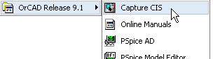
- Go to Start --> Programs -->OrCAD Release 9.1 -->Capture CIS
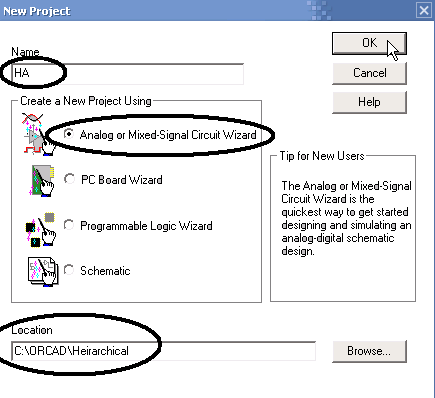
- Go to File -->New -->Project...
- Give a name for your project.
Select Analog or Mixed-signal Circuit Wizard.
Choose a folder for saving your project.
Click on OK.
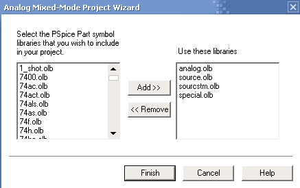
- For digital simulations Add (double click on) 7400.olb (conatins TTL ICs).
For analog simulations Add (double click on) opamp.olb (conatains Op-Amps
including uA741) and diode.olb (contains diodes).
- Now make the circuit in the schematic window.
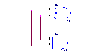
Do not place any input signals or voltage markers yet.
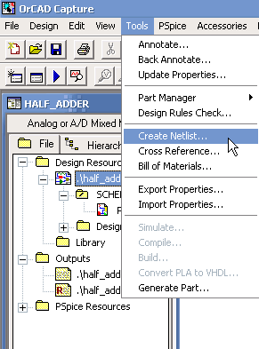
- Now inside the project window, click on the .DSN file under Design
Resources. Now click on Tools à Create Netlist…
- In the dialog box shown below, select the Layout tab; then put a check
mark against Run ECO to Layout; also note down the name of the netlist file (.mnl)
Eg. C:\OrCAD\Half_Adder.mnl.
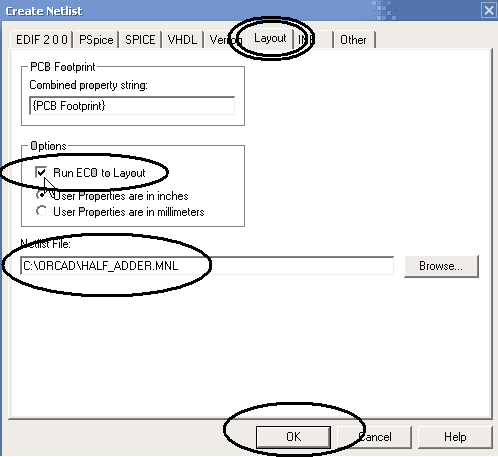
- Click on OK to any message asking you to save.
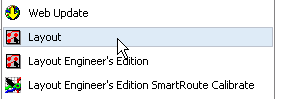
- Close Capture and start Layout from Start -->Programs -->OrCAD Release 9.1
-->Layout
Start --> 
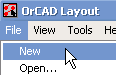
- Open File -->New
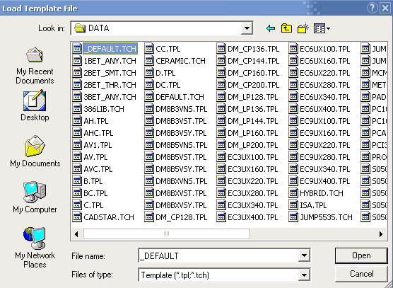
In the Load Template Dialog, select the file :
“C:\Program Files\OrCAD\LAYOUT\DATA\_DEFAULT.TCH”
(Here C: may be D: or any other drive where OrCAD is installed)
- In the Load Netlist Source dialog, browse to the netlist file (.mnl) saved
in step 7.
- In the Save dialog, give any name to save your Layout project. OrCAD will
give the extension .MAX to the board layout file.
- The ECO utility will run and will close automatically if there are no
errors in loading your netlist. Errors may occur if OrCAD does not have the
dimensions of the components you have used in the netlist. Then you can choose
an alternative component of similar size.
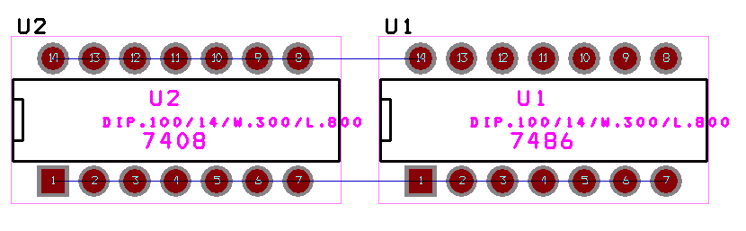
- Now the PCB will appear with all the components (ICs, resistors etc)
placed on it at suitable positions. Any pins to be connected are shown
connected with a yellow line. Initially all of these will be overlapping.
Now click on the Add/Edit Route
 button
the toolbar
button
the toolbar
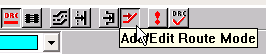 :
:
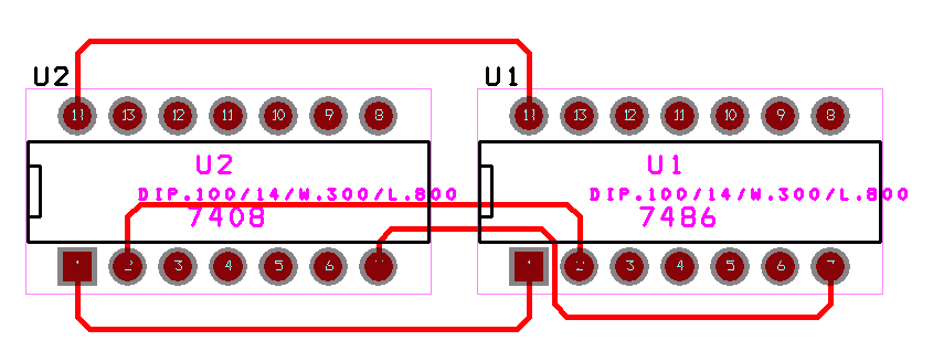
Now you can click on any pin of an IC, if it is connected to any other pin,
both the pins get highlighted. Now you can provide a path between the pins on
the PCB with the mouse.
Click on one pin and click at different points to mark the path towards the
other pin. Clicking on the final pin finishes the path. Make sure you click on
all the pins to see if they are connected.
Make sure that the paths are non-overlapping.
A sample finished PCB layout may look like this:
You can change some settings by opening Options -->Post Process Settings…
There is still some more work to do which is not mentioned here.
Bye.