
Here I present another AT89C2051 programmer with a serial interface. But why
another one when there are so many already around?
The specialty of this programmer is the simple layout which can be easily made
on a general purpose board.
In all the other designs you will find that the Port1 of the "Master" AT89C2051 has to be connected to the Port1 of the "To-be-programmed" AT89C2051 with the same bit ordering, i.e. bit 0 has to be connected with bit 0, bit 1 with bit 1 and so on. Since it is not possible to keep the two AT89C2051s side by side while maintaining the same bit order, you have to carry a lengthy bus and twist it around to reach the other chip.
I decided to change this. If you keep the two AT89C2051s side by side with their top side butted against each other, you get something like this:
You see the pins get all jumbled up, but this is really good for soldering because eight of your connections can now be made directly using solder without any wiring or jumpers on the topside. This jumbling up of the pins can be easily fixed by the software.. which is what I did.
To send a byte to the Port1 of the "To-be-programmed" chip, the master chip
To receive the data, almost a reverse process is used. You can see this in the assembly code.
The serial communication protocol used here is simple, it can even be programmed via hyperterminal, but only if you want to write a few bytes. I do not know how to send a complete file interspersed with write commands using hyperterminal. Anyway, the software I have made is very simple and has not showed up with any problems so far. Here is a screenshot:
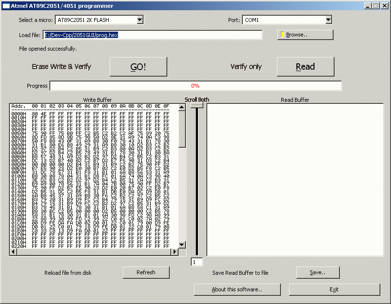
It was developed using the FLTK library and the MinGW gcc compiler. The FLUID tool that is a part of FLTK is a great help in designing interfaces in a fast and easy way. The executable file and source code are provided below in the download section.
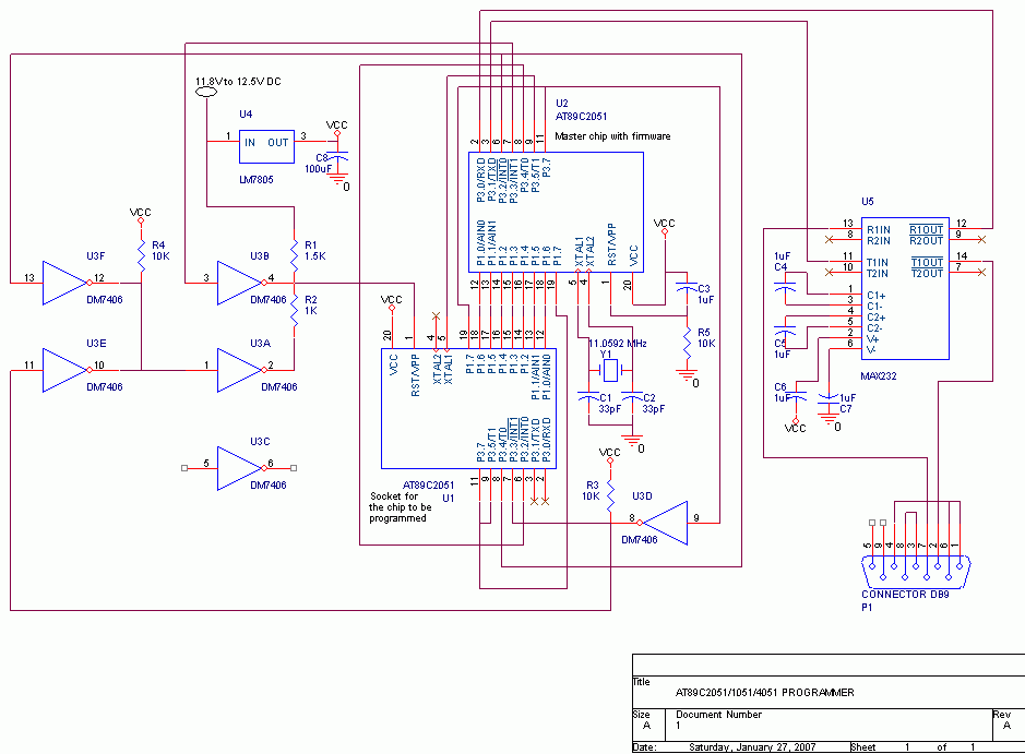
Here are the pictures of the circuit followed by a schematic:

The top side has very few wires moving around. The RS-232 level converter chip MAX 232 is not shown because I have it assembled separately on a small patch board. But in the provided schematic and layout, they are all on the same board sharing the same supply. I have an even better layout in mind, but I have not made it into a board yet.

The bottom side does not have many complex connections either. I may have fumbled up at places, this was the first prototype, but it can be a LOT cleaner. Do check back in for a new and simpler layout. I will post pics too.
And now the SCHEMATIC: (Click here for the Bill of Materials list)
It requires a 12V DC supply. Please check that if the supply is dropping below 11 volts when connected with the circuit, then you need to use a better quality supply with a more reliable output. You can also have a 7812 regulator on board and give a >15V supply. I will put up another schematic using this method soon.
Everything in a single zip file : 2051prog.zip
The contents of the zip file are:
(Note: You can download them individually too by right-clicking on them & choosing save)
prog.asm : Assembly source of the firmware which has to be written to the "Master" chip
prog.hex : HEX file for the above ASM code
schematic.gif : Schematic as a GIF file
schematic.dsn : Orcad design file for the schematic
layout.gif : A possible layout for the circuit (I have not finalized it yet, will put it up once I have built and tested another one)
2051gui.zip : The programmer software executable AND source code
readme.txt : The README file. Contains all the info, including the serial port protocol used.
gpl.txt : The GNU GPL licence
Extra files (Not in the archive, neither required) :
CmdProg.zip : A command line version of the programmer software. This is still a 32-bit windows program, not for 16bit MSDOS.
For the firmware : Since the firmware is in assembly, you can use any 8051 assembler to do the job. I did it with Keil's built in assembler. The hex file is provided anyway.
For the programmer software : It was made using only freely available
tools. My build environment was Dev-C++ IDE with MinGW compiler installed. Plus
I had installed the FLTK2 devpak. Please note - FLTK2, not version 1(even though
version 2 does not have a stable release yet).
I have included the fluid file main.fl so that you can use fluid to modify it,
even though editing the cpp file is also easy. I have used the Intel Hex file
reading code (public domain) by Vanya A. Sergeev to read in the HEX files. You
can also compile it without Dev-C++ which I did most of the time by using the
given makefile, but make suitable modifications to the paths for the include and
lib folders. The Win32 executable files are given.
A port to Linux may not be possible right now, because I have not used the
serial port in Linux. however, by modifying/rewriting the SerialPort class, you
can port it without changing the rest of the program. Happy building.
AT89C2051 Programmer
Copyright (C) 2006  Rohit Rawat

The schematics for the circuit and the source code & executable files
on this webpage are provided for free; you can redistribute them and/or
modify them under the terms of the GNU General Public License
as published by the Free Software Foundation; either version 2
of the License, or (at your option) any later version.

This material is distributed in the hope that it will be useful,
but WITHOUT ANY WARRANTY; without even the implied warranty of
MERCHANTABILITY or FITNESS FOR A PARTICULAR PURPOSE.  See the
GNU General Public License for more details.

You should have received a copy of the GNU General Public License
along with this program; if not, write to the Free Software
Foundation, Inc., 51 Franklin Street, Fifth Floor, Boston, MA  02110-1301, USA