Steps for creating a circuit with hierarchical blocks
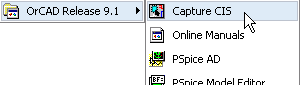
- Go to Start --> Programs --> OrCAD Release 9.1 --> Capture CIS
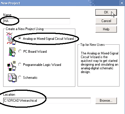
- Go to File --> New --> Project...
- Give a name for your project.
Select Analog or Mixed-signal Circuit Wizard.
Choose a folder for saving your project.
Click on OK.
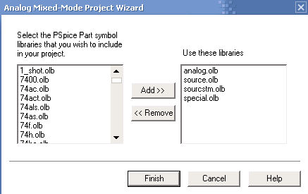
- For digital simulations Add (double click on) 7400.olb (conatins TTL ICs).
For analog simulations Add (double click on) opamp.olb (conatains Op-Amps
including uA741) and diode.olb (contains diodes).
- Now make the circuit in the schematic window. Notice the title of the
schematic window, it says SCHEMATIC1:PAGE1. This means the name of the
schematic is SCHEMATIC1.
Do not place any input signals or voltage markers yet.
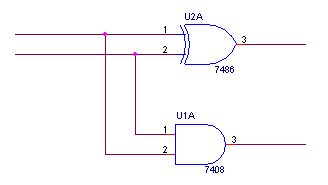
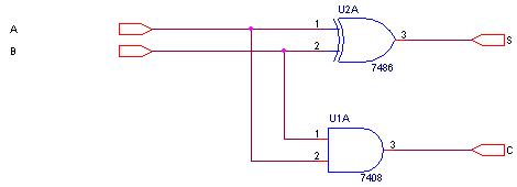
- In the above example of a Half Adder, it has two inputs A and B, and two
outputs Sum and Carry. For each one of them, place a Port using the
Place Port button
 .
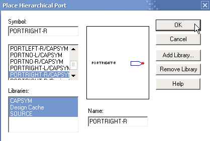
The following dialog appears:
.
The following dialog appears:
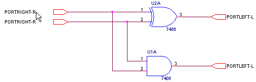
Connect the ports to the inputs and output. For input, the recommended port is
PORTRIGHT-R. For output, the recommended port is PORTLEFT-L.
Double click on the default port names PORTRIGHT-R/L to give them new
meaningful names.
Save the design by clicking on
 .
.
- Open the project window. (Either minimize the schematic window, or choose
Window --> <projectname>).
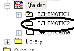
Right click on the .dsn file and chose New Schematic.
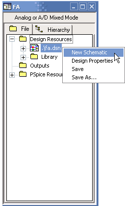
Accept the default name ie. SCHEMATIC2. Notice that it appears under
the .dsn file.
- Now right click on SCHEMATIC2 and click on New Page. Accept the default
name.
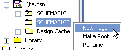
The new page appears under SCHEMATIC2.
Before proceeding, you MUST SAVE NOW by clicking the
button!! Otherwise an error will message will be displayed.
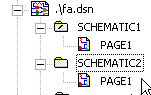
- The SCHEMATIC1 contained the Half Adder that we wanted to use as a
component. We will now use it in the new schematic SCHEMATIC2. But we have to
make SCHEMATIC2 the Root Schematic before we can simulate it. To do this right
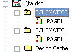
click on SCHEMATIC2 and click on Make Root.
Now the ordering changes and the mark (/) moves from SCHEMATIC1 to SCHEMATIC2.
- Double click on the Page1 of SCHEMATIC2.
The blank schematic page opens.
- Now click on the create hierarchical block icon
 .
.
Fill in any unique name for Reference.
In Implementation Type, select Schematic View.
In Implementation Name, type SCHEMATIC1, i.e. it must be the same as
the one on the Half Adder.
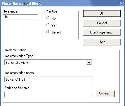
Click OK. Now draw a box in the window with the mouse of any dimensions. The
following will appear:
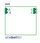
You can drag the ports (A, B, C and D) to comfortable locations within the
block (shown in the last figure).
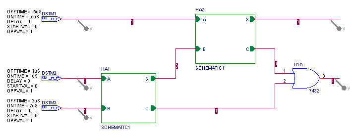
- You can repeat step 12 if you want to put more instances of the block. For
example, we will make a Full Adder with 2 Half Adders, so we have made two
blocks. Keep in mind that reference names should be different like HA1 and
HA2, but the Implementation Name is the same for both the Half Adders:
SCHEMATIC1.
- Now make a circuit with the component blocks and simulate it normally.
Note: If you have problems in placing voltage markers then save, close and
reopen the project.
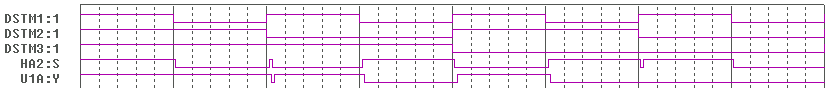
The results are shown:
That’s all folks!